- 您现在的位置:买卖IC网 > Sheet目录624 > HWK60000 (Red Lion Controls)KIT BEZEL WITH PC BOARD & CABLE
�� �
�
�TIME� BASE� SELECTION�
�The� SUB-CUB-R� has� a� time� base� selection� range� of� approx.� 3.9� msec� to� 15.9�
�seconds� in� 3.906� msec� (1/256� second)� increments.� The� minimum� time� base�
�setting� is� obtained� by� pulling� only� the� TB1� input� low� while� the� maximum� time�
�base� is� obtained� by� pulling� all� TB� inputs� low.� Therefore,� a� specific� time� base�
�is� achieved� by� adding� the� appropriate� individual� time� base� increments.� The�
�time� base� increment� total� is� computed� according� to� the� following� formula:�
�DECIMAL� POINT� SELECTION�
�The� selection� of� the� Decimal� Point� is� accomplished� by� the� DPA� and� DPB�
�inputs.� The� table� below� shows� the� logic� states� which� should� be� used� to� obtain�
�the� desired� decimal� point� location.� The� SUB-CUB-R� has� leading� zero�
�blanking.� Note� that� a� change� in� decimal� point� position� will� only� occur� at� the�
�end� of� the� present� time� base� period.�
�WHERE:�
�DR� =�
�DDP� =�
�TIME� BASE� INCREMENT�
�TOTAL� (TBIT)�
�Desired� Reading�
�Display� Decimal� Point�
�=�
�DR x DDP x 15,360�
�RPM� x� PPR�
�DPB�
�Low�
�Low�
�High/Open�
�High/Open�
�DPA�
�Low�
�High/Open�
�Low�
�High/Open�
�D.P.� LOCATION�
�Factory� Test� Mode� Only�
�0�
�0.0�
�0.00�
�RPM�
�PPR�
�DDP:�
�=�
�=�
�Revolutions� Per� Minute�
�Pulses� Per� Revolution�
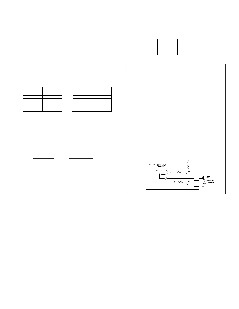
�PULSED� PULL-UP� LATCHED� INPUTS�
�0�
�0.0�
�0.00�
�=�
�=�
�=�
�1�
�10�
�100�
�The� Display� Decimal� Point� (DDP)� value� is�
�determined� by� the� desired� decimal� point�
�placement� in� the� readout.�
�The� Time� base� inputs,� the� Decimal� Point� inputs,� and� the� Frequency�
�Doubling� inputs� are� designed� to� be� actuated� by� wired� or� switched�
�connection� to� Common� or� by� switching� an� open� collector� of� a� transistor� to�
�TIME� BASE�
�INPUT�
�TB1�
�TB2�
�TB3�
�TB4�
�TB5�
�TB6�
�TIME� BASE�
�INCREMENT�
�1�
�2�
�4�
�8�
�16�
�32�
�TIME� BASE�
�INPUT�
�TB7�
�TB8�
�TB9�
�TB10�
�TB11�
�TB12�
�TIME� BASE�
�INCREMENT�
�64�
�128�
�256�
�512�
�1024�
�2048�
�Common.� A� pull-up� resistance� is� provided� for� all� of� these� inputs.� To� keep�
�current� consumption� to� a� minimum,� this� input� circuit� has� been� designed� to�
�latch� the� present� state� of� the� inputs,� allowing� the� pull-up� resistance� to� be�
�switched� on� and� off,� thus� reducing� current� consumption.� The� following� is�
�a� description� of� the� sequence� of� events� for� these� inputs� (Refer� to� the�
�drawing� below):�
�At� the� end� of� a� previous� time� base,� a� 30.5� μsec� pulse� is� generated� within�
�the� time� base� chip� which� will� cause� Q1� to� switch� ON� the� input’s� pull-up�
�EXAMPLE:� Find� the� appropriate� Time� Base� input� settings� for� a� desired�
�display� reading� with� a� fixed� shaft� speed.�
�DESIRED� READING� (DR)� =� 250.0�
�REVOLUTIONS� PER� MINUTE� (RPM)� =� 1250�
�PULSES� PER� REVOLUTION� (PPR)� =� 50�
�resistance.� During� this� time,� if� the� input� is� being� held� low,� the� input� will�
�provide� a� sourcing� current� pulse� thru� Q1.� The� level� of� the� input� (either� low�
�or� high)� is� sensed� by� the� input’s� Latching� Circuit.� When� the� pulse� is�
�terminated,� the� Latching� Circuit� will� hold� the� input� at� its� present� state.�
�If� an� input,� which� is� presently� in� the� high� state,� is� pulled� low,� the�
�Latching� Circuit� will� respond� immediately� and� latch� the� input� in� the� low�
�state.� If� an� input� is� presently� held� in� the� low� state,� and� is� allowed� to� float,�
�TBIT� =�
�250.0 x 10 x 15,360�
�1250� x� 50�
�=�
�38,400,00�
�62,500�
�=� 614.4�
�the� Latching� Circuit� cannot� respond� until� the� end� of� the� time� base;� at� which�
�time,� the� Pulsed� Pull-up� resistance� will� pull� the� input� high.� The� Latching�
�TBIT� =� 614� (round� off� to� the� nearest� whole� number)�
�Circuit� will� then� latch� the� high� state.� A� Master� Reset� (MR)� will� terminate�
�the� present� time� base� and� allow� new� TB� inputs� to� be� latched.�
�TIME� BASE� INPUT�
�REMAINDER� NEEDED�
�TB10� (512)�
�TB7� (64)�
�TB6� (32)�
�TB3� (4)�
�TB2� (2)�
�.........�
�.........�
�.........�
�.........�
�.........�
�614� -� 512� =� 102�
�102� -� 64� =� 38�
�38� -� 32� =� 6�
�6-4=2�
�2-2=0�
�As� shown� above,� Time� base� inputs� TB10,� TB7,� TB6,� TB3,� TB2� are� pulled�
�low� to� generate� the� desired� time� base.� The� actual� time� base� in� seconds� is�
�calculated� by� dividing� the� TBIT� Total� by� 256.�
�614/256� =� 2.398� sec.�
�FREQUENCY� DOUBLING�
�FD� is� the� Frequency� Doubling� input.� When� it� is� in� the� high� state� or� left� open,�
�twice� the� number� of� input� pulses� are� registered� on� the� readout.� This� doubling�
�of� the� signal� input� rate� allows� the� Time� Base� Increment� Total� (TBIT)� to� be�
�halved,� thus� allowing� for� a� faster� update� time� for� a� given� display� value.� If� this�
�input� is� in� the� low� state,� Frequency� Doubling� is� disabled.�
�3�
�发布紧急采购,3分钟左右您将得到回复。
相关PDF资料
HWK70000
CABLE ASSEM FOR MDM SERIES
IF-30-56
XFRMR 115/230V 28V 1.1A 30VA PCB
IL-20-0001
IL5 PULSE TRANSFORMER THT 0.25A
ILR-11-0003
ILR3 IMPULSTRAFO KONVENTIONELL
IS-1000
TRANSFORMER ISOLATION 1000W
IS-250
TRANSFORMER ISOLATION 250W
IS-500
TRANSFORMER ISOLATION 500W
IS1000HG
TRANSF ISO 1000W 4OUT HOSP GRADE
相关代理商/技术参数
HWK6M6
制造商:Hubbell Wiring Device-Kellems 功能描述:CAB, ACCESS,QUADCAB,MTG RAIL KT,M6,2'H
HWK70000
功能描述:CABLE ASSEM FOR MDM SERIES RoHS:是 类别:工业控制,仪表 >> 配件 系列:* 标准包装:1 系列:Aero-Motive® 130117 附件类型:拖车带 适用于相关产品:标准盒式跟踪系统 其它名称:WM6183
HWK9M6
制造商:Hubbell Wiring Device-Kellems 功能描述:CAB, ACCESS,QUADCAB,MTG RAIL KT,M6,3'H
HWKF120
制造商:Hubbell Wiring Device-Kellems 功能描述:CAB, ACCESS,QUADCAB,FAN KT,120VAC
HWKF230
制造商:Hubbell Wiring Device-Kellems 功能描述:CAB, ACCESS,QUADCAB,FAN KT,230VAC
HWKFF
制造商:Hubbell Wiring Device-Kellems 功能描述:CAB, ACCESS,QUADCAB,FAN FILTER KT
HWKGT
制造商:Hubbell Wiring Device-Kellems 功能描述:CAB, ACCESS,QUADCAB,GASKET KT
HWL 160W
制造商:Osram Opto semiconductors 功能描述:Bulk